Schemium Init
Project inception for Schemium (Software Configurable Hardware for Embedded Messaging Interface and Unconstrained Modulation)
Purpose & Intent
I wanted to learn how to make a software defined radio and I got Diwali money that I needed to spend, so I purchased the Z7SDRLite from Hamgeek!! The Z7SDRLite (link to board) is basically a Zynq 7020 that is connected to an AD9363 Radio Frontend. This gives the Zynq the ability to create signals in the fabric and send them to radios!! This is pretty awesome since I know how to use Zynqs really well and I know nothing about radios. So this was going to be great character development. I also decided to document my process of stumbling around because why not, I guess. Anyways the board arrived today finally so lets figure out what is actually here!!! (Also I got the art for the project logo from my favorite card in Lil Alchemist).
First Boot
So I know absolutely nothing about radios so I figured the best thing to do was to plug the board in and see what happens. I found 2 serial ports that openned up on my host and tried the classic 115200 baud. /dev/ttyUSB1 did the trick with the following command bash sudo screen /dev/ttyUSB1 115200 and I was given this output once I logged in with the default credintials I found online (root, analog):
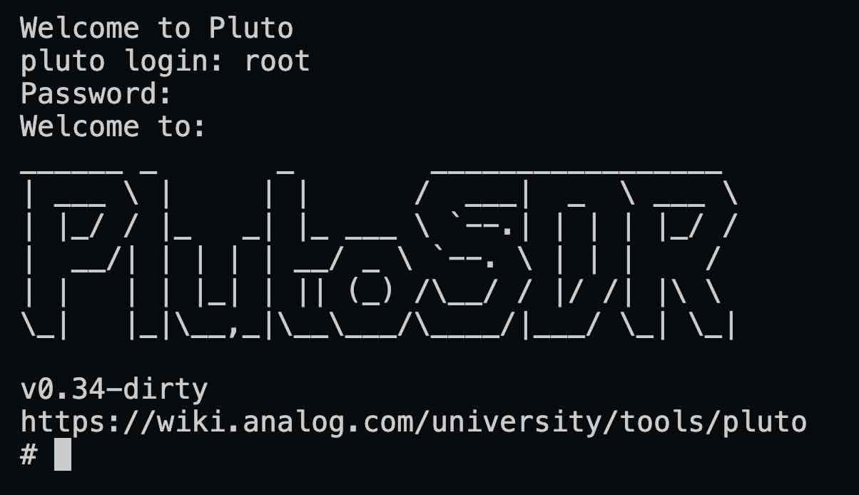 Figure 1: Output from terminal
The Link from login welcome text.
Descent into Madness
So I naturally followed the link to see what documentation I can find and what tutorials I could use. One click lead the another and another until I found myself this awesome repository that contained a bunch of IPs for their products. For those unfamiliar with FPGA development, IPs are basically bundled up logic that can be tossed into an FPGA and connected into a greater design to add a new functionality. I tend to think of them more like libraries for C, where you can include a library and then wire it into your code using a frontend header file. Anyways here is the IP core that I found that is useable for the chip my fpga had on it: link to the repository. Figure 2 is also a block diagram provided by the documentation that shows what the IP is really all about.
 Figure 2: Blcok Diagram
Now this was cool and all, but I had no idea what most of these words meant. I could tell that it looked like I just toss this core into my design and pass it data on the axi streams and manage the core through an axi lite interface, but that didnt explain what an ADC or DAC was. So I went to youtube and found some awesome resouces to better understand what this core even in and get a good idea of what is happening here.
Next Steps
After reading those documents and watching those videos along with other resouces I found online, I gained a small grasp of what was happening, so the next step was to make an project to fuck around with the IP core and find out. I also did never find out what that TDD thing was, I guess I figure it out when I run into it.